What Is Atomic Layer Deposition
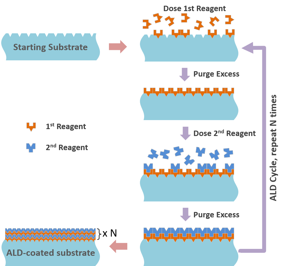
Atomic Layer Deposition (ALD) is a gas phase deposition process based on sequential surface reactions to grow thin films of different materials, wherein the target substrate is exposed, sequentially, to one such reaction at a time.
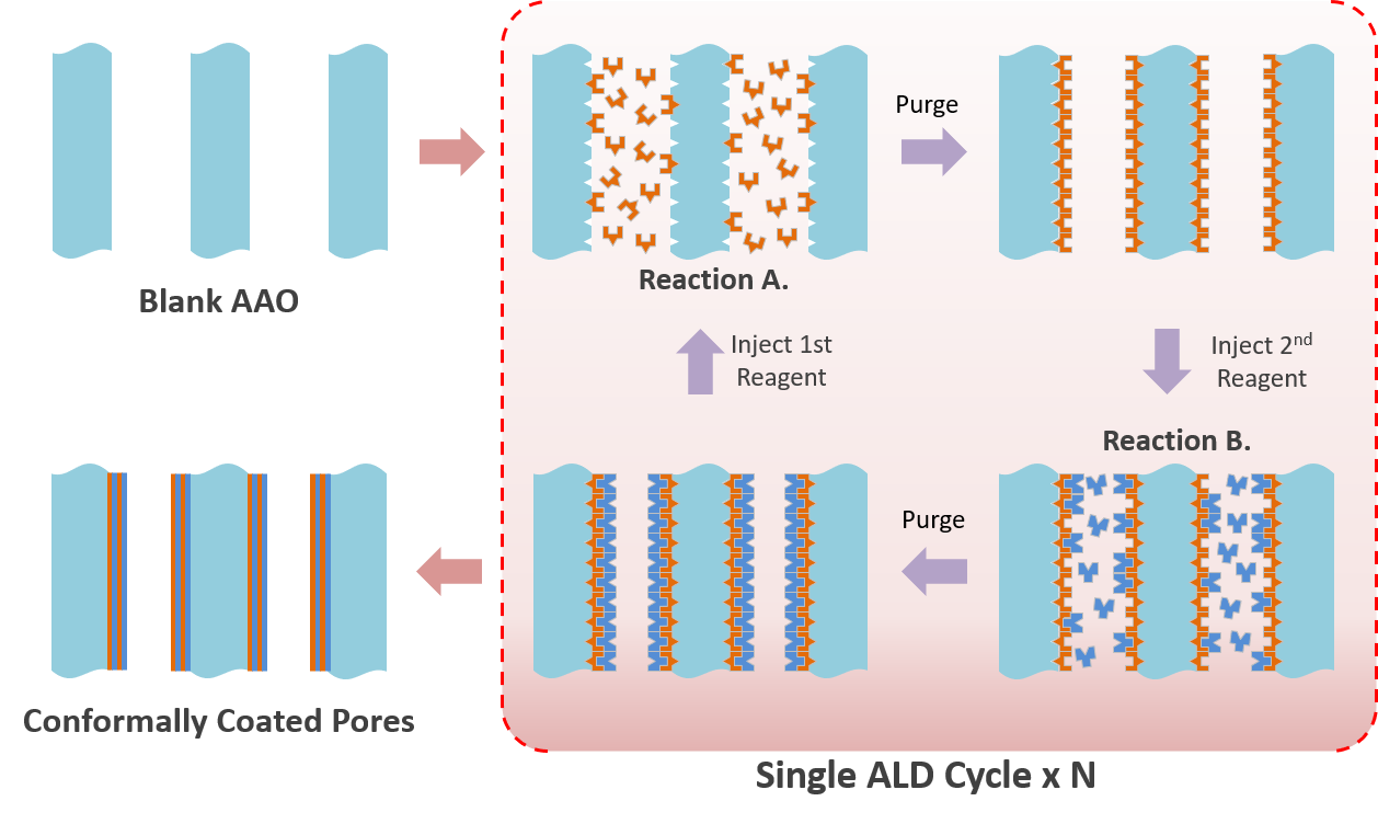
These reactions are surface-limited, with only a monolayer of a given precursor reacting with and/or chemisorbing on the surface. The result is a pinhole free, conformal coating, with superior process control in comparison with other thin film deposition methods, such as Chemical Vapor Deposition (CVD) and Physical Vapor Deposition (PVD).
Key features of ALD that led to its growing applications in the design and fabrication of advanced materials and devices are:
- thickness control with atomic layer accuracy and precision
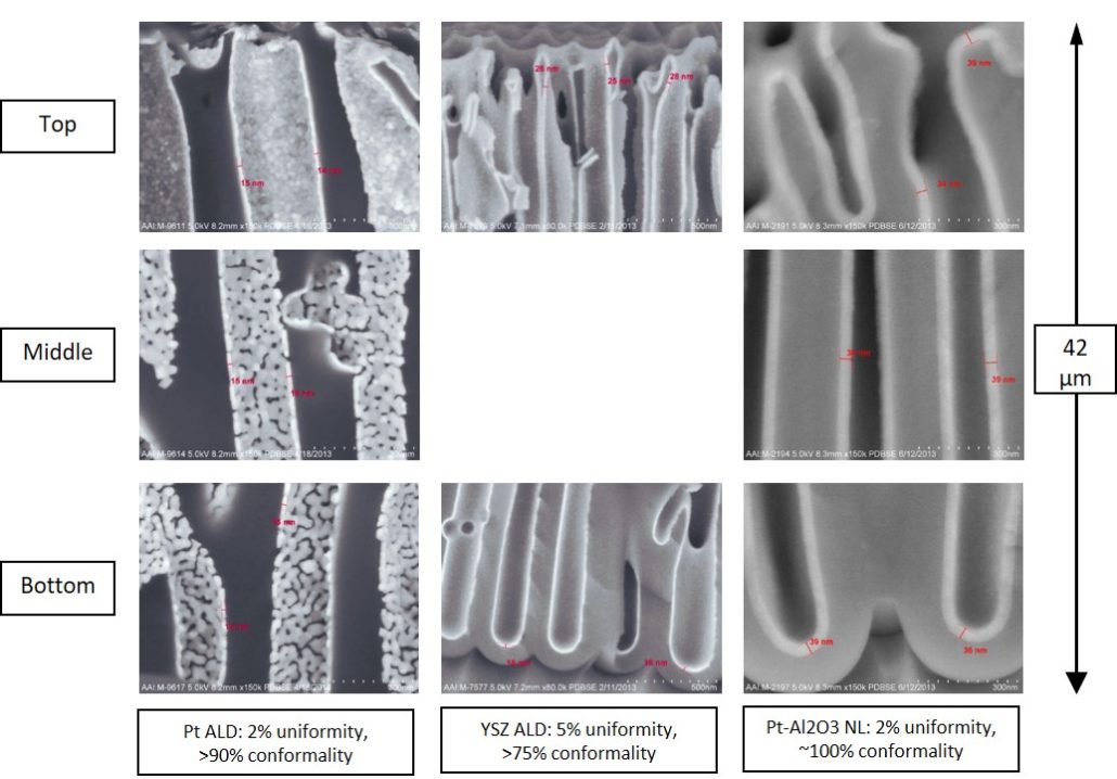
- conformal coverage over high aspect ratio and high surface area materials
- very low defect density with high uniformity
- complex and multilayered films (e.g. nanolaminates, nanoalloys and precise doping)
- a wide variety of insulating, conducting and semiconducting films
Materials Deposited by ALD
ALD of many different materials on flat substrates have been demonstrated.
- oxides, i.e. Al2O3, ZnOx, InOx, TiO2, ZrO2, SiO2, HfO2, Ta2O5, SnO2
- nitrides, i.e. SiNx, TaNx, BN, TiN
- pure metals, i.e. Pt, Ni, Ir, Pd, Ru, Au
- certain polymers.
New processes continue to emerge for ALD of other materials and composites. However, not all of these materials could be easily deployed on high surface area materials with high aspect ratio nanopores. In particular, plasma-based ALD processes are poorly suited as plasma doesn’t penetrate very deep into the pores. On the other hand, thermal ALD processes are more amenable for conformal coatings of high aspect ratio nanopores in materials such as AAO.

An example of partial reactions for ALD deposition of zinc oxide:
(A) ZnOH* + Zn(CH2CH3)2 -> ZnOZnCH2CH3* + CH3CH3
(B) ZnCH2CH3* + H2O -> ZnOH* + CH3CH3
Reagent 1: diethyl zinc Zn(CH2CH3)2 Reagent 2: water vapor H2O


